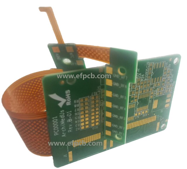
Introduction to HDI PCB: The High-density interstitial copper-embedded PCB
HDI PCBs, also known as High Density Interconnect PCBs, are complex layered printed circuit High-density multilayer PCB boards (CLPCB). These types of boards have become increasingly popular due to their high density and multiple layers structure. They are widely used in various industries such as telecommunications, aerospace, and medical equipment.
Manufacturing Process:
The manufacturing process of HDI PCB involves sever

al steps. Firstly, a thin layer of insulating material is applied on the base substrate. Then, using advanced laser technology or chemical etching methods, intricate patterns and traces are created on the surface of the boa
rd. Afterward, through-hole plating and copper deposition techniques enable the creation of conductive pathways between different layers. To achieve higher density levels, microvias with small diameters are drilled into the board during fabrication.
Characteristics:
HDI PCBs offer numerous advantages over traditional multilayer PCBs. Due to their compact size and densely pac HDI PCB ked components, they require less space compared to conventional circuit boards. This makes them suitable for smaller devices where space optimization is crucial. Additionally, the embedded copper Complex Layered Printed Circuit Board (CLPCB) vias provide improved signal integrity and faster transmission speed.
Advantages:
One major advantage that HDI PCBs offer is increased reliability by reducing electromagnetic interference (EMI) issues caused by signal crosstalk or noise interference between adjacent traces or components. With reduced EMI concerns come enhanced performance capabilities for sensitive electronic systems.
Moreover, these specialized interconnects allow for better thermal management in high-power applications since they can efficiently dissipate heat generated during operation.
Usage Methodolo Multilayer PCB gy:
When using an HDI PCB design approach in new product development projects it’s essential to consider Design for Manufacturability (DFM) analysis early on in the design phase itself.
By involving your High-density interstitial copper-embedded PCB trusted HDI-PCB supplier from concept drawings stage onwards you will be able to leverage their experience in mass manufacturing HDI PCBs and avoid design pitfalls. Supplier input on IPC-2221A; Design Guidelines for Printed Boards Utilizing High-Density Interconnection Technology can be highly beneficial.
Selecting the Right HDI PCB:
When selecting an HDI DFM Analysis PCB for your project, it is crucial to consider your specifi HDI PCB c requirements. Factors such as layer count, via types (microvias or blind vias), material selection, and impedance control must be taken into account. Additionally, working closely with a reliable PCB supplier who offers DFM analysis will ensure that your design is optimized for manufacturability while meeting functional expectations.
Conclusion:
HDI PCBs have HDI PCB revolutionized the electronics industry by enabling smaller devices with higher functionality and improved performance capabilities. Their high-density interconnect technology and embedded copper vias contribute to enhanced signal integrity, reduced EMI issues, and efficient heat dissipation.
When choosing an HDI PCB supplier, it is essen PCB supplier tial to collaborate with experts who provide comprehensive DFM analysis and support throughout the entire manufacturing process. By doing so, you can ensure the successful implementation of HDI PCBs in your innovative designs