Multilayer PCB: Manufacturing Process, Features, Advantages, and Selection Guide
Introduction
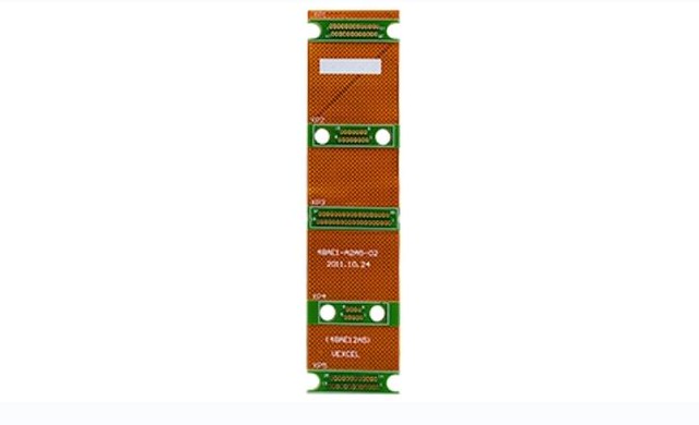
In Flexible PCB the world of electronics and technology, Multilayer PCBs have become an integral part of various devices and systems. This article dives into the manufacturing process, features, advantages, usage methods, and how to select this highly sought-after product.
Manufacturing Process
Multilayer PCBs are designed with several layers of copper traces separated by insulating material known as a substrate. The manufacturing process involves sequential lamination where each layer is aligned precisely on top of another. Once laminated together, these layers undergo etching to create circuitry connections betw Complex PCB een them. Finally, they are coated with a protective sold PCB manufacturer er mask for durability.
Features of Multilayer PCBs
High-density interconnect (HDI) board: With multiple layers packed tightly together using advanced technology.
Complex PCB: Offers intricate design possibilities due to its multi-layered structure.
Multiple-layered PCB: Provides enhanced flexibility in designing complex electronic circuits.
Multi-level PCB: Allows better signal integrity by separating different functional blocks onto different layers.
Multi-layered printed circuit board: Enables smaller form factors without compromising performance or capabilities.
Advantages of Multilayer PCBs
1. Space-saving solution: The compact nature allows engineers to fit Multilayer PCB more components in a limited space.
2. Improved reliability: Multiple copper layers strengthen connectivity without risking damage or interference from external High-density interconnect (HDI) board sources.
3. Enhanced performance: Reduced electromagnetic interference keeps signals cleaner and minimizes crosstalk between neighboring traces.
4. Cost-effective production: Although initially costly due to complex manufacturing processes involved; it saves money in the long run through improved functionality and reduced maintenance needs.
Usage Methods for Multilayer PCBs
1. Communication Systems:
– Routers
– Switches
– Wireless transmitters/receivers
2 Multilayer PCB . Automotive Industry:
– Engine control units (ECUs)
– Anti-lock braking systems (ABS)
– Infotainment systems
3. Medical Equipment:
– Ultrasound machines
– Patient monitors
– MRI scanners
4. Industrial Applications:
– Control systems
– Automation equipment
How to Select Multilayer PCBs
1. Determine the required number of layers based on circuit complexity and space constraints.
2. Consider the size, wei Multiple-layered PCB ght, and dimensions of the final product.
3. Assess material specifications like substrate type, copper thickness, and insulation properties to ensure compatibility with your needs.
4. Evaluate the manufacturing capabilitie PCBA Coating s and quality assurance processes of different PCB manufacturers or suppliers.
5. Request samples to test performance, reliability, and durability before committing to bulk orders.
Conclusion
Multilayer PCBs have revolutionized electronic device manufacturing by providing high-density interconnectivity in a compact form factor. With their complex design options and improved f Multilayer PCB unctionality compared to traditional single-layer boards, they offer numerous benefits across various industries such as communication systems, automotive technolog

y, medical equipment, and industrial applications. When selecting multilayer PCBs for your specific requirements, it is crucial to consider factors like layer count, size constraints, material specifications while assessing the expertise of potential suppliers in producing reliable and top-quality PBC products.