Title: The Advantages of HDI PCBs in Modern Electronics
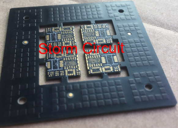
In the world of modern electronics, Hi HDI PCB gh-Density Interconnect (HDI) printed circuit boards have become increasingly popular due to their advanced technology and compact design. HDI PCBs, also known as Microvia PCBs Multilayer PCB or Fine-line printed circuit boards, are a type of High-density interstitial copper-embedded PCB that offer numerous benefits for various applications.
Manu HDI PCB facturing Process:
HDI PCBs are manufactured using a complex process that involves multiple layers of copper interconnects with microvias that are laser-drilled for maximum precision. This allows for a higher density of connections within a smaller surface area, making them ideal for compact electronic devices such as smartphones and tablets.
Characteristics: Fine-line printed circuit board
These types of PCBs have finer lines and spaces which contribute to their high density and compact size. The use of microvias also reduces signal distortion and improves overall signal integrity in high-sp Microvia PCB eed applications.
Advantages:
One key advantage of HDI PCBs is their ability to reduce the size and wei PCB supplier ght of electronic devices without compromising on performance. They also offer better thermal performance due to improved heat dissipation capabilities. Additionally, HDI PCBs can support multiple functions within the same board, reducing the n
eed for additional components.
How to Use:
When designing with HDI technology, it is important to consider Design For Manufacturability (DFM) Analysis. This ensures that the manufacturing process will be efficient and cost-effective while meeting all necessary sp

ecifications.
Choosing an HDI PCB Supplier:
When selecting an HDI PCB supplier, it is crucial to look for experience in producing high-quality products with tight tolerances. A reliable supplier should also offer comprehensive HDI printed circuit board DFM analysis services to op HDI PCB timize your design for manufacturability.
Conclusion:
Overall, HDI PCB technology offers significant advantages in terms of size reduction, improved performance, and enhanced functionality in modern electronic devices. By choosing the right sup DFM Analysis plier and understanding how to leverage these benefits through proper design techniques, businesses can stay ahead in today’s competitive market.