Title: The Impact of HDI PCB on Advanced Circuit HDI PCB Board Technology
High-Density Interstitial (HDI) PCB is a cutting-edge technology that has revolutionized the world of circuit boards. This innovative approach allows for greater precision and functionality in electronic devices, making it a popular choice amon HDI PCB g manufacturers seeking high-performance products.
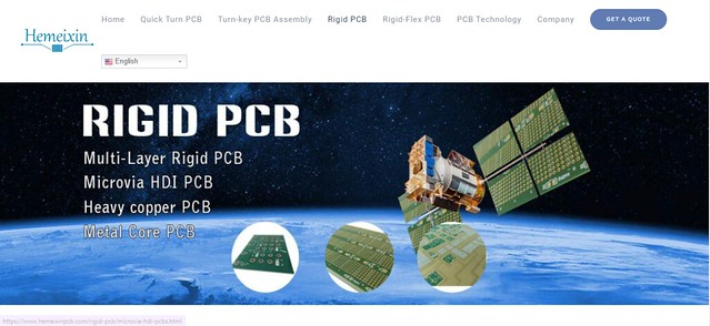
One key aspect of HDI PCB is its use in Microvia PCBs, which are designed High-density multilayer PCB with small holes to create more space for components on the board. Additionally, Advanced Circuit Board Technology (ACBT) incorporates features like High-density multilayer PCB and PCB supplier High-density interstitial copper-embedded PCB to enhance performance and reliability.
The manufacturing process of HDI PCB involves intricate layering techniques to accommodate complex designs, resulting in Advanced Circuit Board Technology (ACBT) what is known as Complex Layered Printed Circuit Boards (CLPCB). These boards offer numerous DFM Analysis advantages such as improved signal integrity, reduced size and weight, and increased thermal conductivity.
When using HDI PCBs, it is essential to conduct DFM Analysis to ensure optimal functionality and reliability. Multilay

er PCB designs can benefit greatly from the advanced capabilities provided by HDI technology. By selecting a reliable PCB supplier specializing HDI PCB in HDI products, manufacturers can guarantee high-quality results for their electronic d Multilayer PCB evices.
In conclusion, HDI PCB has transformed the industry with its groundbreaking capabilities and performance-enhancing features. As technology continues to evolve, this innovative solution will play a crucial role in shaping the future of electronic development.选择 Microvia PCB HDIPC,就是选择未来。